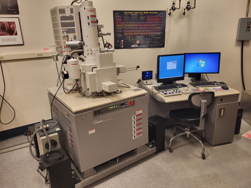
HITACHI S-4800 FIELD EMISSION SCANNING ELECTRON MICROSCOPE (FE-SEM)
Location: Egan Research Center, Room 106
Status: Operational
Booking: Priority Software® FBS
Description: Hitachi S-4800 FE-SEM is a high-resolution scanning electron microscope (SEM) with cold field emission gun. It is equipped with the energy-dispersive X-ray spectroscopy (EDS) system (EDAX detector and Team software) that enables elemental analysis. It also has a Nabity nanolithography e-beam pattern generation system.
Instrument Specifications:
| Electron Source | Cold Field Emission Gun |
|---|---|
| Accelerating Voltage | 500V to 30kV in 100V steps |
| Resolution | 1.0 nm Accelerating Voltage 15kV, Working Distance 4 mm 2.0 nm Accelerating Voltage 1kV, Working Distance 1.5 mm |
| Magnification | High Mag Mode 100x to 800,000x Low Mag Mode 30x to 2,000x |
| Specimen Stage | X Traverse 0 to 110 mm Y Traverse 0 to 110 mm Z Traverse 1.5 to 40 mm Tilt -5° to +70° Rotation 360° |
| Specimen Size | Max. 150 mm (6″) |
| Image Mode | Secondary Electron Imaging Back Scattering Electron Imaging |
| Accessories | EDAX system with Teams software |

______________________________________________________________________________________________________________________________
TESCAN VEGA 3 LMU VARIABLE PRESSURE SCANNING ELECTRON MICROSCOPE (VP-SEM)
Location: Egan Research Center, Room 429
Status: Operational
Booking: Priority Software® FBS
Description: TESCAN VEGA 3 LMU variable pressure scanning electron microscope (VP-SEM) has a thermionic-W electron source and suitable for imaging solid or semi-liquid samples. It is equipped with an Oxford energy dispersive spectrometer (EDS) for sub-micron spatial resolution elemental analysis and an Oxford electron backscatter diffraction (EBSD) system for in situ mineralogical and crystallographic analysis of biomineralized structures. The system also supports rapid mapping of elemental composition and crystallographic orientations.
| Electron Source | Tungsten heated cathode |
|---|---|
| Accelerating Voltage | 200 eV to 30 keV |
| Resolution | High Vacuum Mode (SE): 3 nm at 30 kV / 2 nm at 30 kV 8 nm at 3 kV / 5 nm at 3 kV Low Vacuum Mode (BSE, LVSTD): 3.5 nm at 30 kV / 2.5 nm at 30 kV |
| Magnification | 2x – 1,000,000x (for 5’’ image width in Continual Wide Field/Resolution) |
| Specimen Stage | Type: Compucentric, fully motorized Movements: X = 80 mm (–40 mm to +40 mm) Y = 60 mm (–30 mm to +30 mm) Z = 47 mm Rotation: 360° continuous Tilt: –80° to +80° Maximum Specimen Height: 54 mm (with rotation stage) 81 mm (without rotation stage) |
| Probe Current | 1 pA to 2 uA |
| Image Mode | Resolution: High-resolution mode Depth: Sets the column up in a mode that enhances depth of focus Field: Optimizes the column to provide a large non-distorted field of view Wide Field: Provides an extra-large non-distorted field of view for extra low magnification imaging Channeling: Working mode for assessment of crystal orientation data of the specimen, acquiring of electron channeling pattern (ECP) |
| Accessories | OXFORD EDS & EBSD systems with Aztec software |
